IBM unveils breakthrough 2nm chip technology
The 2nm architecture promises much longer battery life for devices as well as drastic performance boosts


Sign up today and you will receive a free copy of our Future Focus 2025 report - the leading guidance on AI, cybersecurity and other IT challenges as per 700+ senior executives
You are now subscribed
Your newsletter sign-up was successful
IBM has revealed the design for the world’s first 2nm chip in a breakthrough the firm claims will vastly improve energy efficiency and performance of various kinds of devices.
This innovation is projected to achieve 45% higher performance or 75% lower energy use than today’s most advanced 7nm variations, IBM says. Benefits will be felt across a variety of appliances, from consumer and enterprise tech to critical infrastructure systems.
IBM claims the 2nm chips can quadruple the battery life of smartphones, slash the carbon footprints of data centres, and drastically speed up a laptop’s functions. They can also contribute to faster object detection in autonomous vehicles.
“The IBM innovation reflected in this new 2 nm chip is essential to the entire semiconductor and IT industry,” said Darío Gil, SVP and director of IBM Research.

“It is the product of IBM’s approach of taking on hard tech challenges and a demonstration of how breakthroughs can result from sustained investments and a collaborative R&D ecosystem approach.”
Although IBM bowed out of the semiconductor market in 2014, its research and development division has been exploring chip innovation ever since. IBM Research maintains a good track record in the space, having previously been the first to implement the 7nm and 5nm process technologies, among other computing innovations.
RELATED RESOURCE

The smart buyer’s guide to flash
Find out whether flash storage is right for your business
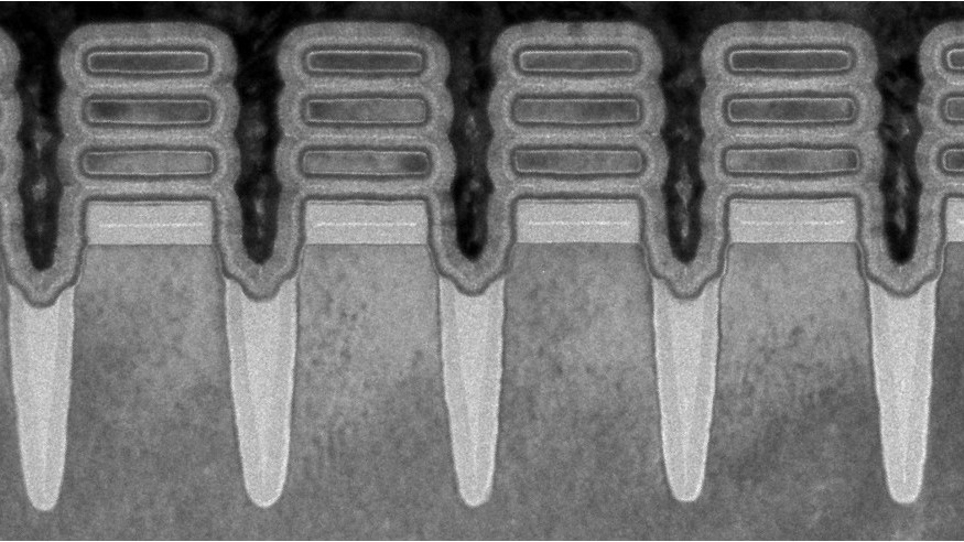
The 2nm design demonstrates the advanced scaling of semiconductors using IBM’s nanosheet technology, the company says, which was a new type of transistor developed after its 5nm chip breakthrough in 2017.
Sign up today and you will receive a free copy of our Future Focus 2025 report - the leading guidance on AI, cybersecurity and other IT challenges as per 700+ senior executives
This architecture will allow the 2nm chip to fit up to 50 billion transistors on a chip the size of a fingernail. More transistors will give designers more options to infuse core-level innovations to improve the capacity for workloads such as artificial intelligence (AI) or cloud computing.
The news is timed roughly six weeks after IBM announced a collaboration with Intel on advanced semiconductor research and development. The two tech giants will collaborate to advance next-generation logic and packaging technologies, with these efforts boosting semiconductor manufacturing.
It's unclear at this stage whether Intel's efforts fed into the development of the 2nm chip design, or whether the partnership means Intel will be among the first to reap the benefits in terms of semiconductor manufacturing.

Keumars Afifi-Sabet is a writer and editor that specialises in public sector, cyber security, and cloud computing. He first joined ITPro as a staff writer in April 2018 and eventually became its Features Editor. Although a regular contributor to other tech sites in the past, these days you will find Keumars on LiveScience, where he runs its Technology section.
-
 Anthropic announces big tech partnership to test new Claude Mythos AI model
News Anthropic’s Project Glasswing will give a host of leading tech companies access to its new Claude Mythos model for testing
-
 Anthropic pens multi-gigawatt TPU deal with Google and Broadcom as Claude demand picks up
News The frontier model maker is looking to greatly expand its compute infrastructure to meet surging customer demand
-
 Nvidia’s Intel investment just gave it the perfect inroad to lucrative new markets
News Nvidia looks set to branch out into lucrative new markets following its $5 billion investment in Intel.
-
 The US government's Intel deal explained
News The US government has taken a 10% stake in Intel – but what exactly does the deal mean for the ailing chipmaker?
-
 US government could take stake in Intel as chip giant's woes continue
News The move would see increased support for Intel’s manufacturing operations
-
 Dell says Windows 11 migration is a prime opportunity to overhaul ageing PC fleets – and AI devices are in the spotlight
News The shift to Windows 11 means IT leaders can ditch old tech and get their hands on AI PCs
-
 The gloves are off at Intel as new CEO plots major strategy shift
News Intel’s incoming CEO has some big plans for the firm’s business strategy, sources familiar with the matter have told Reuters, with more job cuts looming on the horizon.
-
 Intel just won a 15-year legal battle against EU
News Ruled to have engaged in anti-competitive practices back in 2009, Intel has finally succeeded in overturning a record fine
-
 AMD and Intel’s new x86 advisory group looks to tackle Arm, but will it succeed?
News The pair will look to make x86 CPU architecture more interoperable
-
 Why the world is about to be swamped with AI PCs
News With adoption rates set to surge, AI PCs will become far more mainstream in years to come