


-
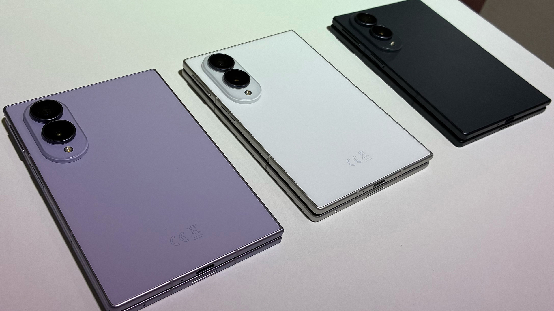 Samsung tests new shapes and materials for a more durable and immersive Galaxy Z Fold 8 line-up
News A new titanium structure reinforces the Samsung Galaxy Z Fold 8 Ultra, while the standard 8 sports a 3:4 ratio for more immersive content consumption
-
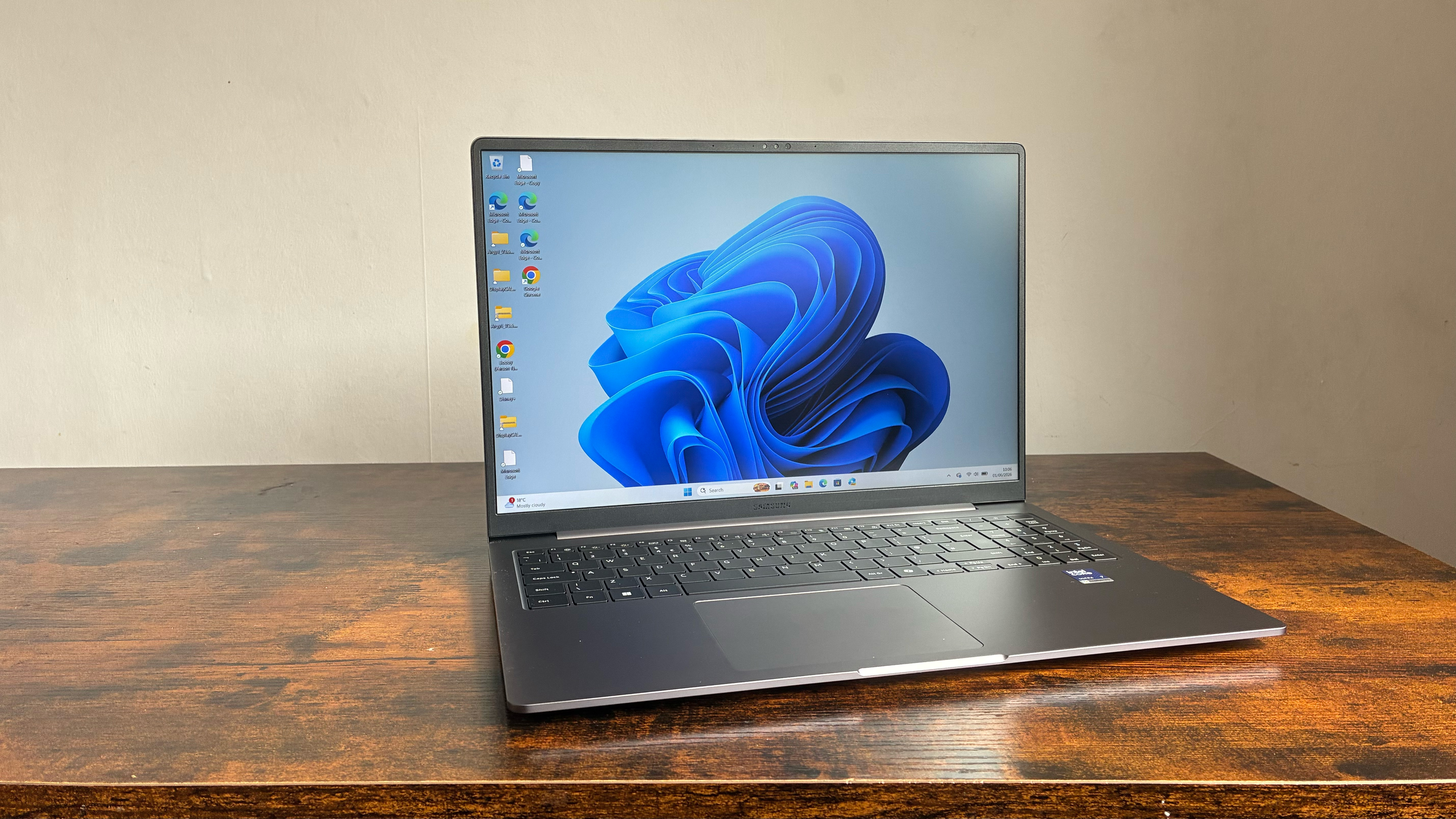 The Samsung Galaxy Book6 Enterprise Edition will make life easier for IT departments – and they'll love the battery life
Reviews A powerful, yet reliable laptop, but the real pull is the Enterprise features that ease deployment and remote management
-
 AMD and Samsung forge closer ties on AI memory, potential foundry deal
News The pair are forging closer ties on chip development and future foundry opportunities
-
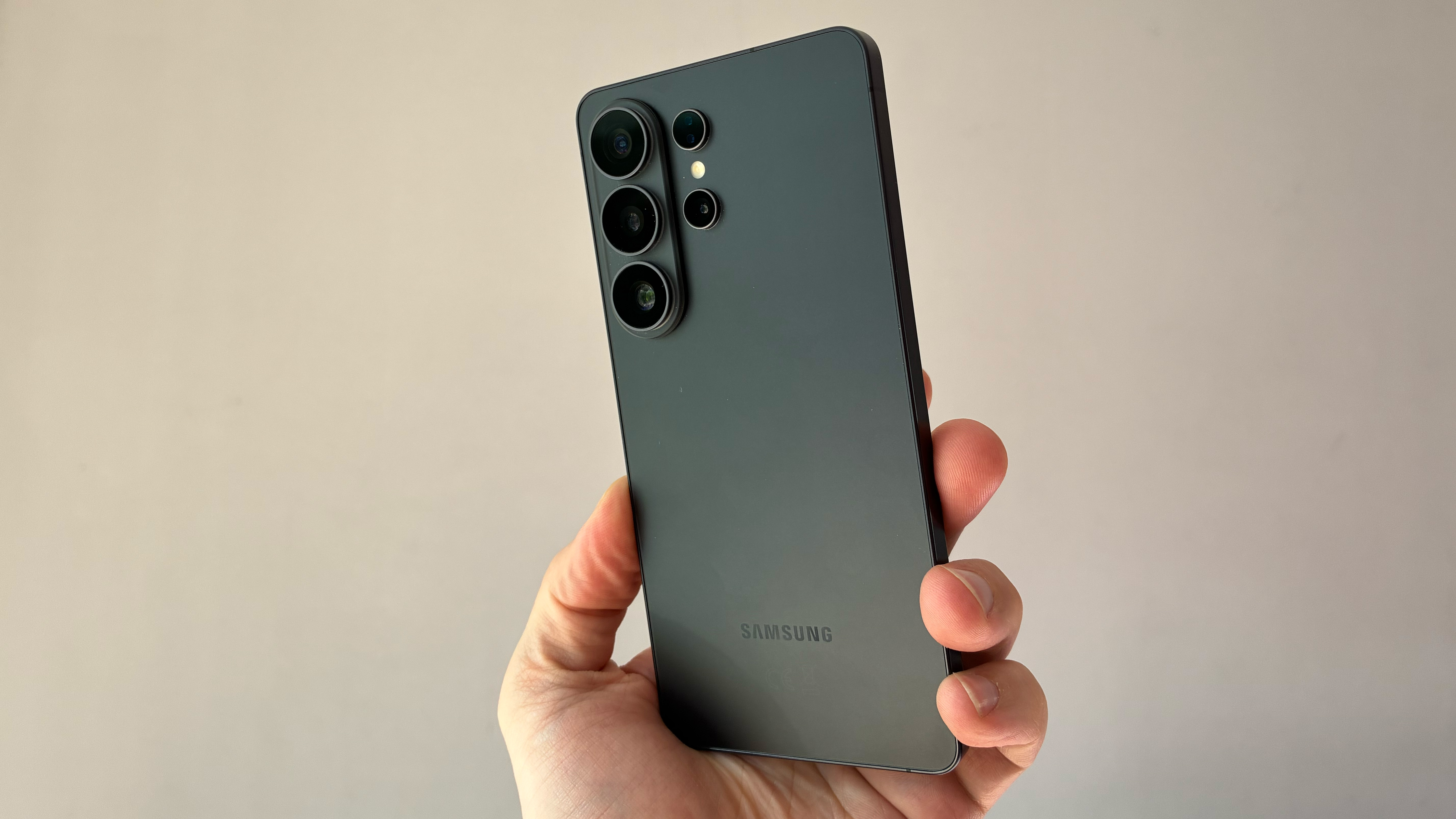 The Samsung Galaxy S26 Ultra is almost an all-in-one solution for video production – its stabilization capabilities are out of this world
Reviews A big, beautiful slab of a smartphone with a cutting-edge privacy display and video capabilities for all your creative needs
-
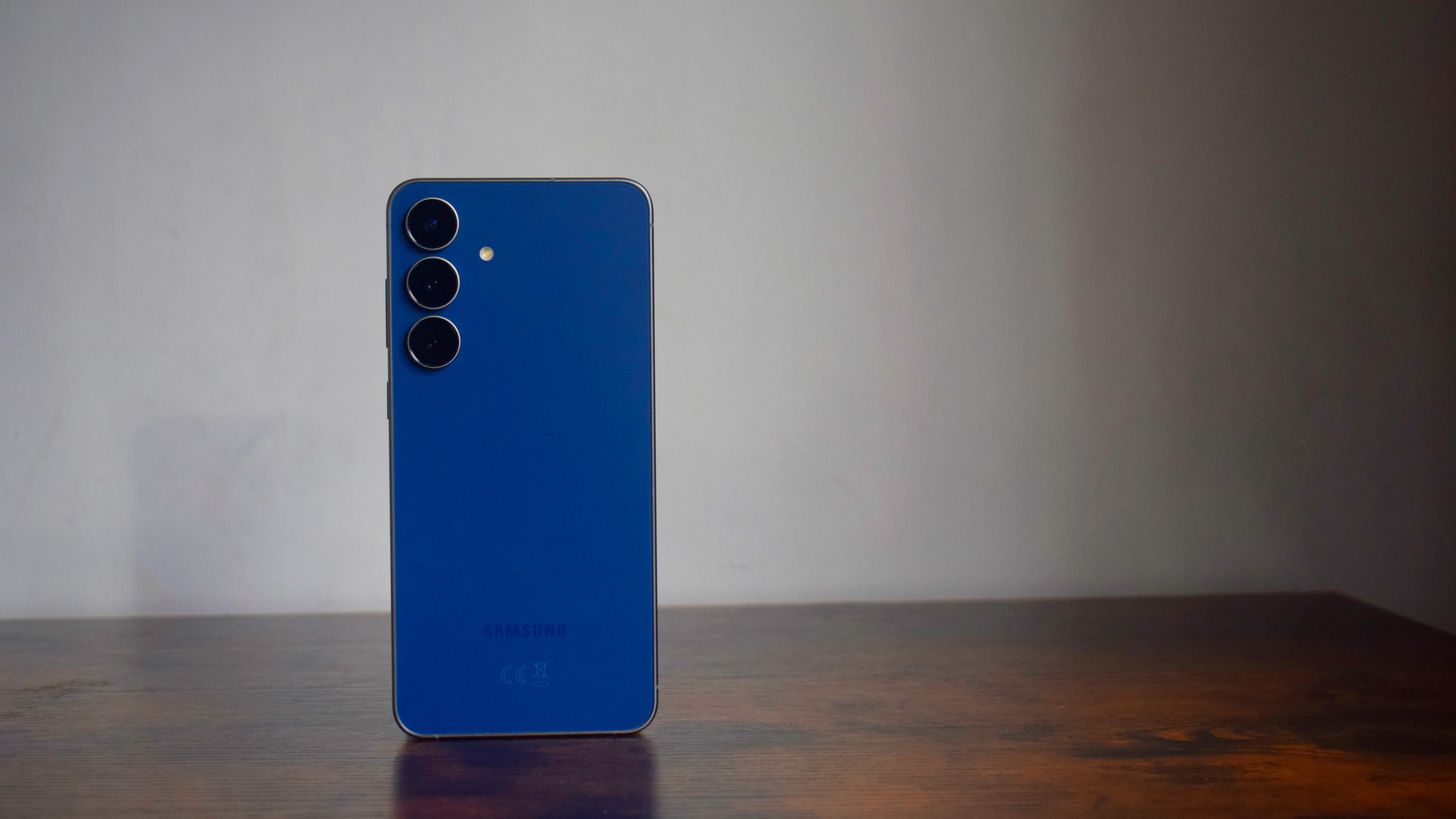 The Samsung Galaxy S25 FE is a superb budget smartphone with premium features – though I found its predictive text frustrating
Reviews A big bright display, all-day battery, and some super premium cameras make this a superb handset for office bods
-
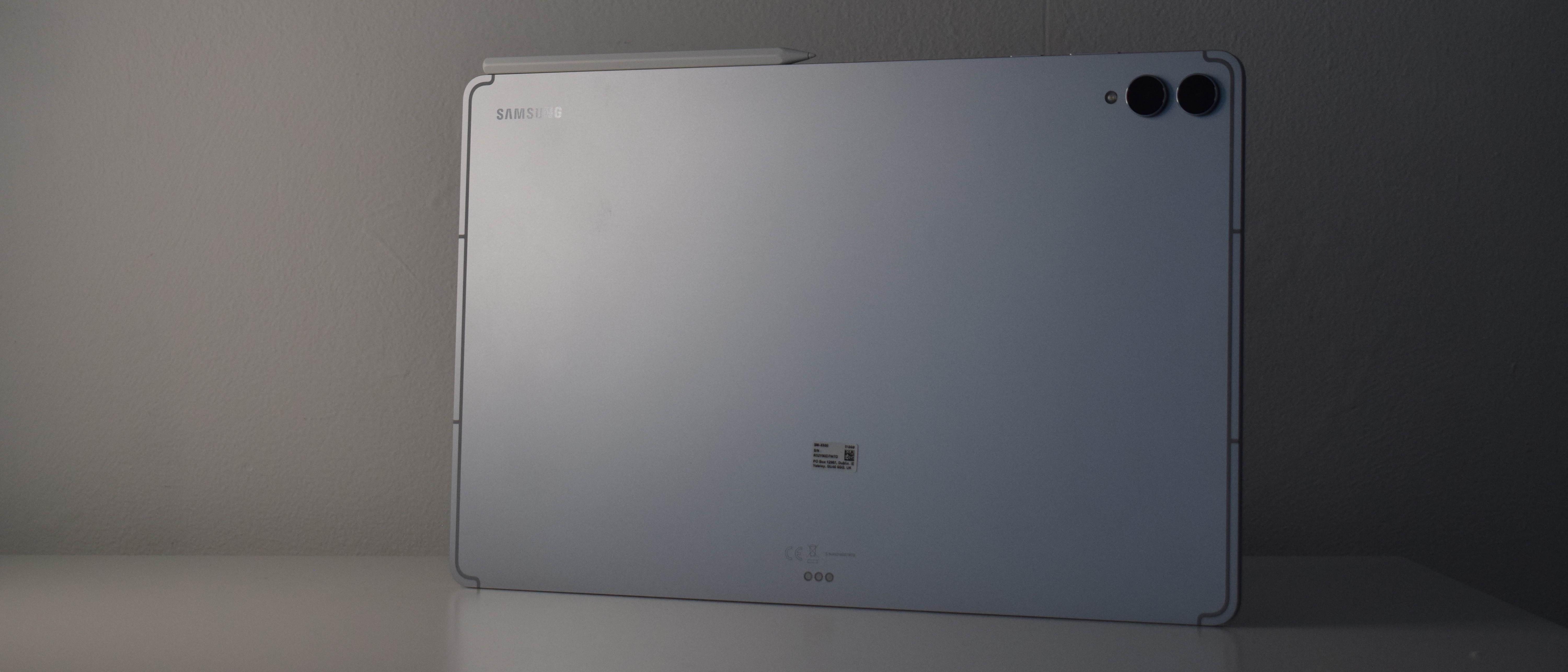
 The excellent Samsung Galaxy Tab S11 is slightly overpriced
Reviews A brilliant lightweight tablet with a superb screen, but the competition makes it look expensive
-
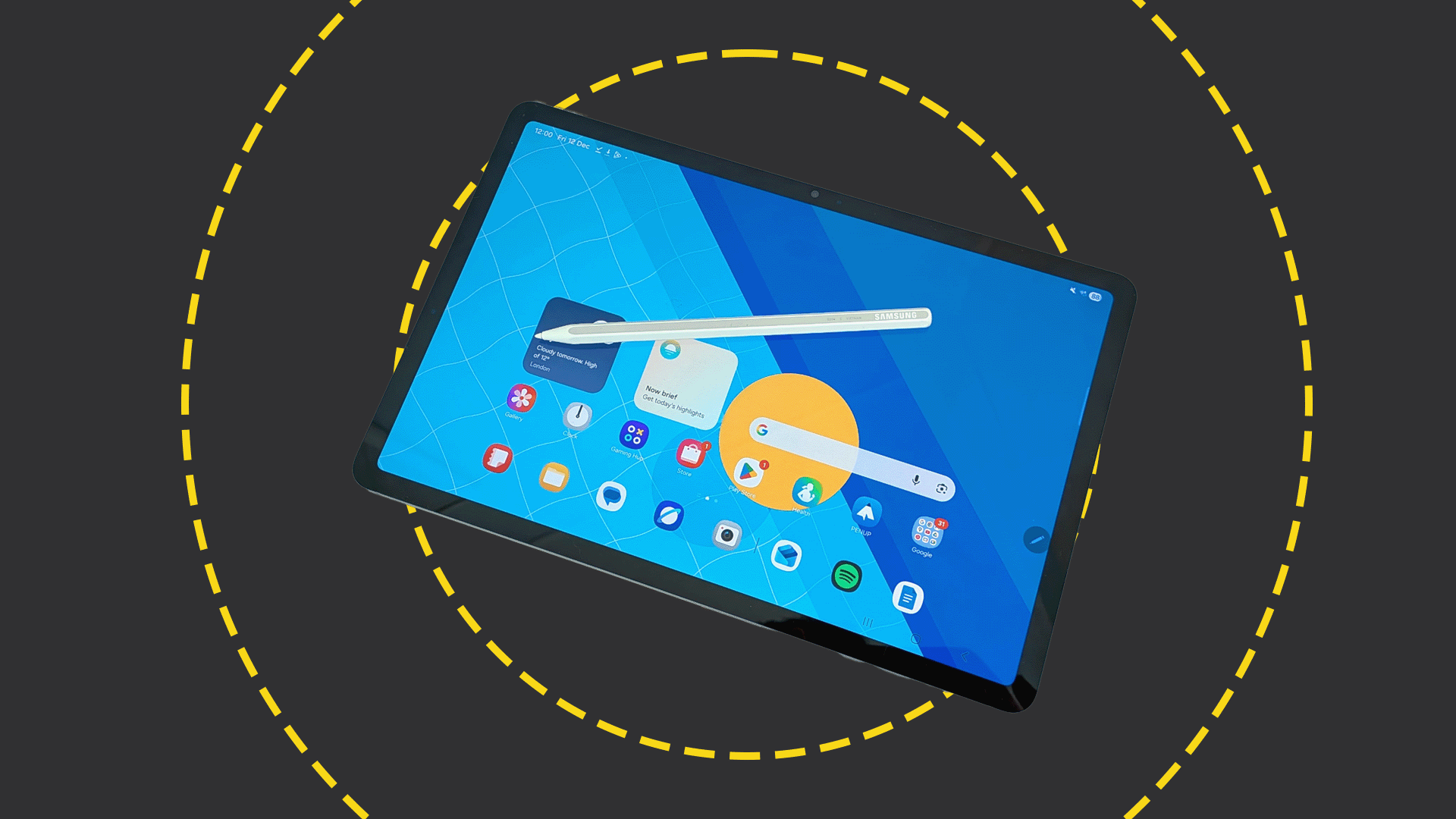
 The Samsung Galaxy Tab S11 Ultra has more power, more AI, and much more battery life than its predecessor
Reviews A wonderful slab of technology, packed with AI features, and the battery life is fantastic – very much a tablet worthy of the name, 'Ultra'
-
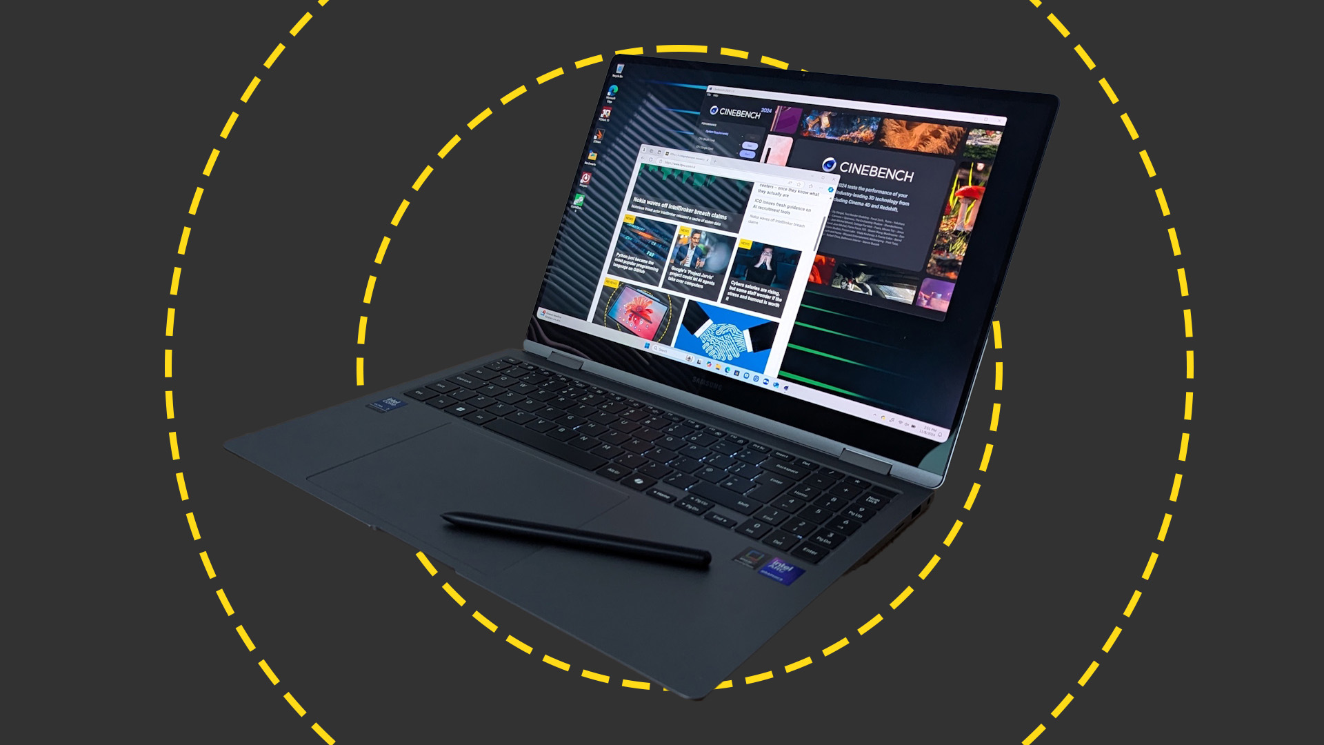 Samsung Galaxy Book 5 Pro 360 review: Almost the perfect big-screen laptop
Reviews The Book 5 Pro 360 is a laptop you slowly get accustomed to, rather than one that feels right from the word go.


